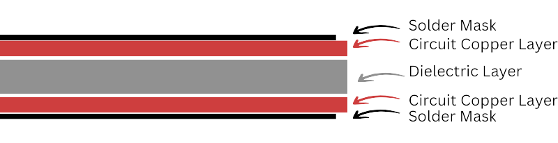
Double Layer PCB
A double-layer PCB (printed circuit board) is a type of circuit board that has two layers of conductive material, typically copper, separated by a non-conductive material called the dielectric layer. The two layers are typically connected together via plated through-holes also known as vias, which are drilled through the dielectric layer. The top layer is typically used for routing signals, while the bottom layer is used for power and ground connections. This allows for more efficient use of space and can also provide shielding for sensitive signals.
Benefits of Double Sided PCBs
- More Flexible to Design
- Increased Circuit Compactness
- Relatively Cost-Effective
- Transitional Level of Circuit Density
- Compact Board Size (which can reduce costs)
PCB Specifications Table
| SR |
SPECIFICATIONS |
STANDARD |
| 1 | Minimum conductor width | 6 mils (0.15 mm) |
| 2 | Minimum conductor spacing / Air gap | 6 mils (0.15 mm) |
| 3 | Minimum plated hole size | 16 mils (0.4 mm) |
| 4 | Maximum plated hole size | 240 mils (6 mm) |
| 5 | Maximum board size | 300 mm x 350 mm |
| 6 | Maximum number of layers | 2 |
| 7 | Minimum copper thickness | 1 Oz (35 microns) |
| 8 | Maximum copper thickness | 3 Oz (105 microns) |
| 9 | Dedicated Electrical Testing (BBT) | Available |
| 10 | PCB Cutting options | Routing, V-groove, Punching |
PCB Surface Finish and Masking Specifications
| SR |
SPECIFICATIONS |
STANDARD |
| 1 | Single Sided | HAL, Lacquer |
| 2 | Double Sided | HAL, TIN, Electroplated Gold & Nickel |
| 3 | Solder Mask Finish | PISM, Liquid Solder Mask |
| 4 | Solder Mask Color | Green, White, Black, Blue, Red |
| 5 | Legend/Ident Color | White, Black, Yellow, Green |
| 6 | Special Requirement | Carbon Printing on Push Button, Selective Gold & Nickel plating on Connecting Tabs |
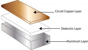
PCB Metal
PCB Technical Specifications
| SR |
SPECIFICATIONS |
STANDARD |
| 1 | Minimum conductor width | 6 mils (0.15 mm) |
| 2 | Minimum conductor spacing / Air gap | 6 mils (0.15 mm) |
| 3 | Minimum plated hole size | 16 mils (0.4 mm) |
| 4 | Maximum plated hole size | 240 mils (6 mm) |
| 5 | Maximum board size | 300 mm x 350 mm |
| 6 | Maximum number of layers | 2 |
| 7 | Minimum copper thickness | 1 Oz (35 microns) |
| 8 | Maximum copper thickness | 3 Oz (105 microns) |
| 9 | Dedicated Electrical Testing (BBT) | Available |
| 10 | PCB Cutting options | Routing, V-groove, Punching |